
“Drawing is not only a way to come up with pictures: drawing is a way to educate your eye to understand visual information, organizing it into a more hierarchical way, a more economical way. When you see something, if you draw often and frequently, you examine a room very differently.” -Vik Muniz
If you've ever wired something up yourself and successfully hit that switch for the first time, you know what that sense of magic feels like. Have a listen to Forest City Lovers as they sing about that same feeling in a different context,
while you consider how maddening circuit building can be.
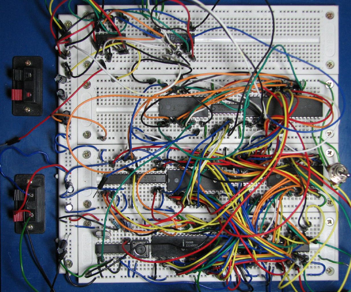 Image credit: © Michael Richmond at RIT, via http://spiff.rit.edu/classes/phys312/workshops/w10c/chips/chips.html.
Messing with loose wires is the bane of a great many physics students and teachers, from the first, basic levels of schooling all the way up through high school, college and even graduate school. Breadboards aren't as much help as you want them to be (and can often even add an extra layer of confusion), and going from the idea of a complete circuit to a true working circuit often proves elusive.
Until, that is, now.
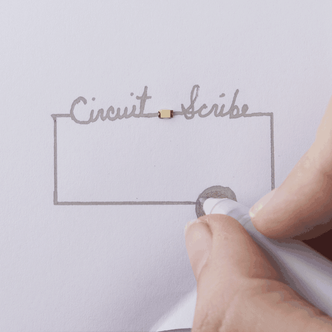 Image credit: Circuit Scribe’s Kickstarter, via https://www.kickstarter.com/projects/electroninks/circuit-scribe-draw-c….
Have a look at Circuit Scribe, which allows you to literally draw your own electronic circuits!
For the simplest of circuits, this appears to be a good introductory method of learning basics. However, even for the LED circuit, the silver deposit is acting as a current limiting element of the circuit. If a student were to hard-wire that same setup, he (she) would not have a LED to play with for very long. Current drawn by the LED should be limited to 10 -15 mA for best performance, so the silver trace is going to get rid of the rest of the current available as heat.
As for anything more complicated (taking the photo of the breadboard as an example), the penned tracks will not function as required. Given the resistance of the ' ink ' is about 10 ohms per inch, only the slowest of logic circuits MAY function with some success.
There is still no substitute for hard wiring a project. From this method, one learns patience, care in layout, the true value of components associated with the circuit, and the opportunity to fine-tune the function of the circuit. If the process requires a PCB, then most of the layout has been achieved during construction of the breadboard / ratsnest / deadbug styles of creation.
As a teenager I remember drawing resistors with a pencil. Graphite works similarly to the silver ink used here, only the resistance is a lot higher. Also I discovered that if you put higher voltage across them micro-arcs form between the graphite particles, which at best changes the resistivity, at worst the paper plus resistor catches on fire.
Good, healthy way to discover ..... :)
as long as you didn't burn the house down in the process.
The pen is nifty, but for kit packages designed to teach concepts I've been a bigger fan of the Snap Circuits product.
https://www.youtube.com/watch?v=JyWdmkK0_U8
For prototyping I am old school and use perfboards with thru-hole components. If it all works then etching your own PCBs and switching to surface mount components isn't that tough. It would be interesting to see if the ink in the Circuit Scribe pen could function as a 'no-solder' solder paste for surface mount components on PCBs.
Cute video, just for kids.
Think you would have a problem with the ' ink ', though. It's not capable of holding much down when dry, unless you smother the connection point. Any flexure & the stuff cracks away.
Definitely stick to the dotted matrix - 0.1 pitch copper pads - double sided. Been using it for 30 odd years; never fails.
Getting the younger generation interested, well, that's another issue. Seems most young folk would rather have ready-made goods instead of using what they have to achieve their goal.
@PJ #5
I've also made good use of learning to solder, but I can see why it is a dying skill. Pick-and-place machines are insanely fast. Here's a video of one placing and soldering 500 components in just over 90 seconds.
https://www.youtube.com/watch?v=nah4BQ9y8IY
That kind of manufacturing efficiency combined with the internet's ability to find just about anything makes doing anything yourself hard to justify unless you like tinkering.
@Denier #6 and PJ #5: It's certainly true that ultra-high-speed pick-and-place machines have done wonders for mass manufacturing. What's interesting is that the CNC and 3D printing "revolutions" are making pick-and-place manufacturing accessible to desktop users. CNC machines are available which can fabricate PCBs, and 3D printers can handle highly conductive "inks" (much better than CircuitScribe!) which can lay down traces on those same just-made PCBs.
There is a very strong and vibrant DIY community which is more than just "people who like tinkering." Look at Kickstarter, and see how many of the fabrication products (as opposed to art or music stuff) were either prototyped, or actually being manufactured, using at-home CNC milling, 3D printing, and circuit building. Look at MAKE Magazine, the Instructables Web community, Etsy, and on and on.
@Michael Kelsey #7
Interesting! I did not even think they had 3D Printers cranking out PCBs. How do boards constructed from relatively low melting point 3D printer resin hold up to soldering?
@Denier #8: I don't believe PCBs as such are created using 3D printing. Rather, you can use a desktop CNC mill to shape the raw board material (e.g., G10), including drilling accurate placement holes for components and vias, then put the board into a 3D printer with a conductive "filament" for printing both the circuit traces and component pads.
There are even printers which can do multi-filament printing with both structural and conductive materials (see the EX1 and Voxel8, for example), reducing the need for PCBs as such.
There are even some new multi-head devices coming out, where you can use software to switch the heads themselves, converting the same x-y-z device from a 3D printer to a CNC mill to a pick-and-place.
The future isn't quite here yet, but it's close...
For home assembly, nothing beats hand/eye co-ordination. The desktop P&P machines are very slow still. One has to set up each component pretty well individually. I suppose for a more complicated circuit it could be a boon.
Isolation routers are quite the help for home PCB manufacture. I have a converted Roland plotter I use as an isolation router. Quite nifty when it comes to a final product.
Even have a 3D printer - managed to print quite a few telescope parts for my projects. A 4 axis CNC is the next cab off the rank.
But then, I am a DIY sort of guy.
;)
@PJ #10: Awesome! I absolutely wasn't claiming that the desktop machines were mass-production level. But five or ten years ago they didn't even exist!
I tried, several years ago, to do some really simple SMD assembly at my work (after 5:00 pm, needed to replace a blown cap, blah blah blah), and came very close to throwing the board and everything on it through a wall. I don't know how our techs can do that...
Yes, I realize you weren't. I have been keeping an eye on a couple of products that claim such advances, until you read the bottom line. I have a full production line P&P at my disposal, but, by the time it is programmed, stocked & run, I've usually finished my project already. Maybe when we get down to 0201 sized components (heh,heh).
I guess we each have our special niche for what we enjoy. I get a thrill out of making my own equipment - design through to finished item. Some enjoy the theoretical sciences as obviated by this site. :)
@Michael Kelsey #9
Michael Kelsey wrote:
After doing some research it seems the conductive filament has non-trivial resistance. Interesting stuff for sure, but the technology has a ways to go before it displaces rapid prototyping houses like 3PCB.com.
The 3D printer that has me drooling is the MarkForged - Mark One. I loathe working with epoxy so a printer that would let me print carbon fiber reinforced composite components has a lot of interest.
This is nice, but conducting ink-jet color has been around for years. :)
@Sinisa Lazarek #14
After researching, it looks like there are several types of conductive ink. There is one video on making the ink used by CircuitScribe, but the interesting part of the video was how he used it; On foam board using thru-hole components.
https://www.youtube.com/watch?v=mF_Z8RUZjJE
There is even one spot in his layout where he uses a trace-hopping wire bridge to get around the single layer 2D limitation.
I'll still stick to my methods. That was sooooooo messy. I'll give him an A for adaptation, though.
I was pretty successful using 12 inch alligator clip wires on IC component socket leads hanging in mid air. But things start to fall apart after about a year. ;-P
Perf board lasts longer.